

At a recent keynote in Shanghai for the 2026 IEEE International Symposium on Circuits and Systems (ISCAS), Huawei announced a brand-new architecture designed to get around current chip manufacturing bottlenecks, and they even put forward a new scaling law to replace the ageing Moore’s Law.
Moore’s Law (named after Gordon Moore, Intel’s co-founder) is the observation that the number of transistors in an integrated circuit (IC) doubles about every two years, with minimal increase in cost.
For over five decades, Moore’s Law has pretty much dictated how the chip manufacturing industry operates. Lately, though, it has been hitting a bit of a brick wall due to physical limits and shrinking economic returns, mostly because it relies so heavily on geometric scaling.
To tackle this, Huawei came up with a new approach called the Tau Scaling Law. This law replaces transistor size with the time constant τ (Tau) as the primary metric for measuring progress.
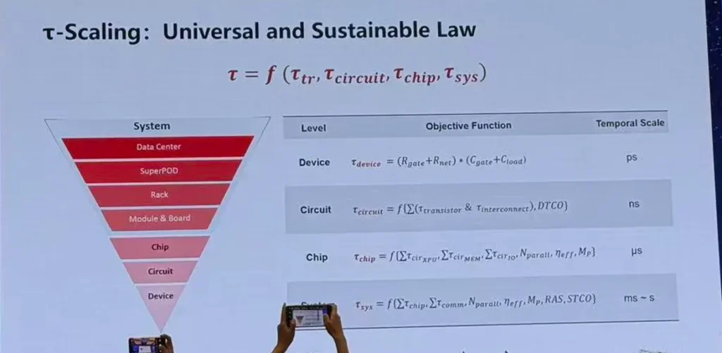
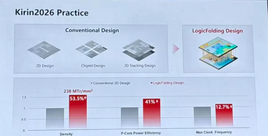
Huawei has already mass-produced 381 chips using this new law across a bunch of different industries. Alongside the Tau Scaling Law, they also developed a new LogicFolding architecture. This new tech constantly compresses signal propagation delay and bumps up transistor density, and it can be used for everything from basic circuits and systems to advanced chips.
Huawei’s next-generation 2026 Kirin smartphone chips will be the first to feature the LogicFolding architecture, promising a massive performance leap over older models when they hit shelves in Fall 2026.
Looking further down the road, Huawei is already planning for 2031, promising high-end chips with a transistor density equivalent to a cutting-edge 1.4nm process.