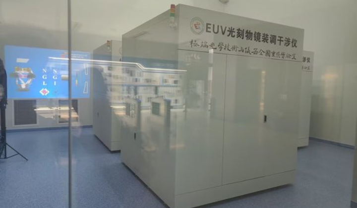
China’s domestic development of extreme ultraviolet (EUV) lithography is advancing rapidly, with Huawei testing a new system at its Dongguan facility that uses laser-induced discharge plasma (LDP) technology.
EUV is used in the semiconductor industry to manufacture integrated circuits (ICs) by creating intricate patterns on silicon wafers using extremely short wavelength light to produce highly detailed, powerful microchips.
According to TechPowerUp, this innovative approach generates 13.5 nm EUV radiation by vaporising tin between electrodes and converting it to plasma via high-voltage discharge, offering advantages such as simplified architecture, improved energy efficiency, and potentially lower costs compared to Advanced Semiconductor Materials Lithography’s (ASML) laser-produced plasma (LPP) method.
The system is set for trial production in Q3 2025, with mass production targeted for 2026, potentially challenging ASML’s monopoly in advanced lithography.
The LDP method contrasts with ASML’s LPP approach, which relies on high-energy lasers and complex control systems. While ASML has decades of refinement in LPP technology, China’s LDP system could accelerate its catch-up in semiconductor manufacturing, especially after U.S. sanctions limited access to EUV tools.

Huawei’s EUV machine aims to upgrade older deep ultraviolet (DUV) systems, which previously constrained domestic chip production. Leading fabs like Semiconductor Manufacturing International Corporation (SMIC) are collaborating with Huawei to integrate the new EUV scanners into existing workflows, though the full impact of this development remains to be seen.
If this goes well, ASML’s High-NA EUV tools, priced at around USD380 million (~RM1.67 billion), face potential competition from China’s more cost-effective alternative.

